We use cookies to enhance your browsing experience, serve personalized ads or content, and analyze our traffic. By clicking "Accept All", you consent to our use of cookies.
We use cookies to help you navigate efficiently and perform certain functions. You will find detailed information about all cookies under each consent category below.
The cookies that are categorized as "Necessary" are stored on your browser as they are essential for enabling the basic functionalities of the site. ...
Necessary cookies are required to enable the basic features of this site, such as providing secure log-in or adjusting your consent preferences. These cookies do not store any personally identifiable data.
No cookies to display.
Functional cookies help perform certain functionalities like sharing the content of the website on social media platforms, collecting feedback, and other third-party features.
No cookies to display.
Analytical cookies are used to understand how visitors interact with the website. These cookies help provide information on metrics such as the number of visitors, bounce rate, traffic source, etc.
No cookies to display.
Performance cookies are used to understand and analyze the key performance indexes of the website which helps in delivering a better user experience for the visitors.
No cookies to display.
Advertisement cookies are used to provide visitors with customized advertisements based on the pages you visited previously and to analyze the effectiveness of the ad campaigns.
No cookies to display.
Challenging traditional approaches, xyztec’s dedicated R&D team has developed many innovative technologies that provide a variety of ways to improve bond testing. Some of these developments are protected by patents, granted in Europe, the United States of America, China, Taiwan and/or other territories. Among these are:
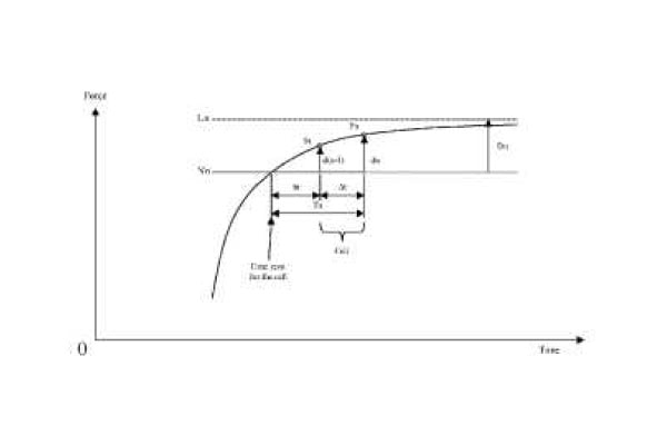
Sensor apparatus for determining a deformation due to creep in an output of a sensor, said sensor apparatus comprising force means arranged for applying a mechanical force to said sensor, said sensor arranged for measuring, in a current measurement, a displacement of said sensor caused by said applied force and a processor component arranged for determining said deformation due to creep for a next measurement by said sensor.
Links: BPP eRegister, Espacenet
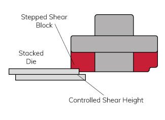
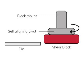
A test device for shear testing semiconductor die bonded to a substrate. Shear block being self aligning and made from a soft material to minimise stresses on the die caused by the test load thereby reducing or eliminating any damage to the die. Different block designs can be made to suit different applications, shear face being tailored to test either single die, die placed very closely to each other or stacked die. The depth of shear face may be less than the die thickness ensuring that the bond surface is not damaged by block during the test.
Links: Espacenet, Google, EP-register, BPP eRegister.
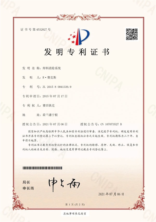
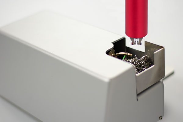
The present invention provides a method of cleaning solder from the jaws of a solder ball test device. The method comprising the steps of heating a gas to a temperature above the melting temperature of the solder and directing the heated gas over the jaws of a solder ball test device to remove solder from said jaws. An apparatus which for carrying out the method is also disclosed.

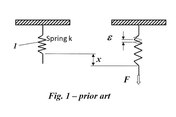
A method for testing a bond using a bond tester apparatus, the method comprising the steps of applying a mechanical force to the bond, determining, by a sensor component comprised by the bond tester apparatus, the applied force to the bond by measuring, by the sensor component, a displacement of the sensor component caused by the applied force and calculating, by the sensor component, the applied force on the basis of a first component which comprises a direct relationship with the measured displacement and on the basis of at least one of a second component, a third component and a fourth component.
Links: Espacenet, Patentscope

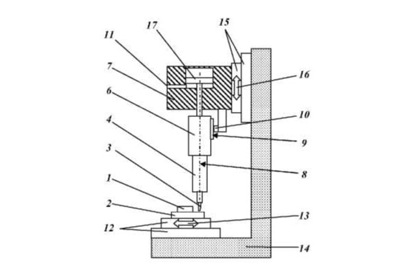
A bond tester apparatus arranged for determining a strength of a bond and/or a material present on a base, said bond tester apparatus comprising a force measurement module for applying a shear force to said bond and/or said material, and a displacement module and a controller arranged for controlling the distance between the force measurement module and the displacement module such that the shear height of a shear tool can be set.
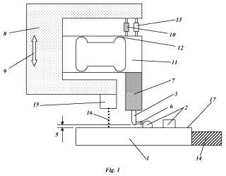
A method of calibrating a sensor of a materials tester, wherein said sensor is arranged to measure a shear force applied by a tool of said materials tester to a sample, for example a wafer or a printed circuit board, said materials tester comprising a shear sensor mount, wherein said sensor is mountable on said shear sensor mount, wherein said method comprises the steps of accelerating said shear sensor mount over a predefined distance towards and/or away from said sample; measuring, by said sensor, a relative movement of said shear sensor mount; calibrating said measured relative movement to an acceleration of said shear sensor mount, thereby testing operation of said sensor.
Links: Espacenet
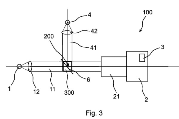
A system for determining a the distance from tool to camera in a work area of a bond tester, comprising: – a light source positioned sidewards of the work area, configured to emit a light beam for illuminating the tool from the side; – a camera, positioned sidewards of the work area across of the light source, arranged to capture images of the light source and the tool; – a processor, communicatively coupled with the camera and configured for processing images received from the camera, wherein in use the tool is positioned within the light beam that is emitted from the light source to the camera, and wherein the processor is configured to determine positioning data of the tool by evaluating local differences in light intensity on the images captured by the camera while viewing the light source and the tool.
Links: Espacenet
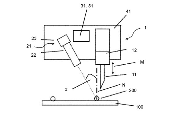
A bond tester, for testing a characteristic of a bond between a substrate and an element bonded to said substrate, the bond tester comprising: – a tool configured to be in contact with the element during a test cycle, the tool moveable towards and away from the element to be tested; – a positioning camera, for viewing the substrate through a lens thereof, and – a processor, arranged in communication with the positioning camera for receiving images taken by said camera, the processor configured for determining a position of the tool relative to the element based on said images, wherein the camera effectively views the substrate at an angle compared to a direction normal to the substrate, allowing the camera to view both the element to be tested and the tool when the tool is in a position near or in contact with the element.
Links: Espacenet
Several other xyztec patents have not been published yet.
J.F. Kennedylaan 14b
5981 XC
Panningen
The Netherlands
Am Haupttor / Bürocenter
06237
Leuna
Germany
27182 Burbank
Foothill Ranch
CA 92610
United States
72/7 M.12 Soi. Soonthornwipak
Bangpla, Bangphli,
10540 Samut Prakan
Thailand
No. 157, Zhongzheng
6th St., Hukou
Township, Hsinchu
County 303,
Taiwan (R.O.C.)
Room 2012
Haichuang Mansion,
No.288 Dengyun Road,
High-tech district, Kunshan,
Jiang Su, China
Xyztec develops world-class bond testing technologies and works together with global partners to provide local support worldwide.
J.F. Kennedylaan 14b
5981 XC
Panningen
The Netherlands